


Semiconductor manufacturing depends on more than wafer processing. The equipment used for deposition, etching, inspection, testing, handling, and clean production also relies on carefully engineered parts. For buyers, the practical challenge is turning a drawing or early prototype into repeatable, clean, and traceable equipment components.
The route in one view
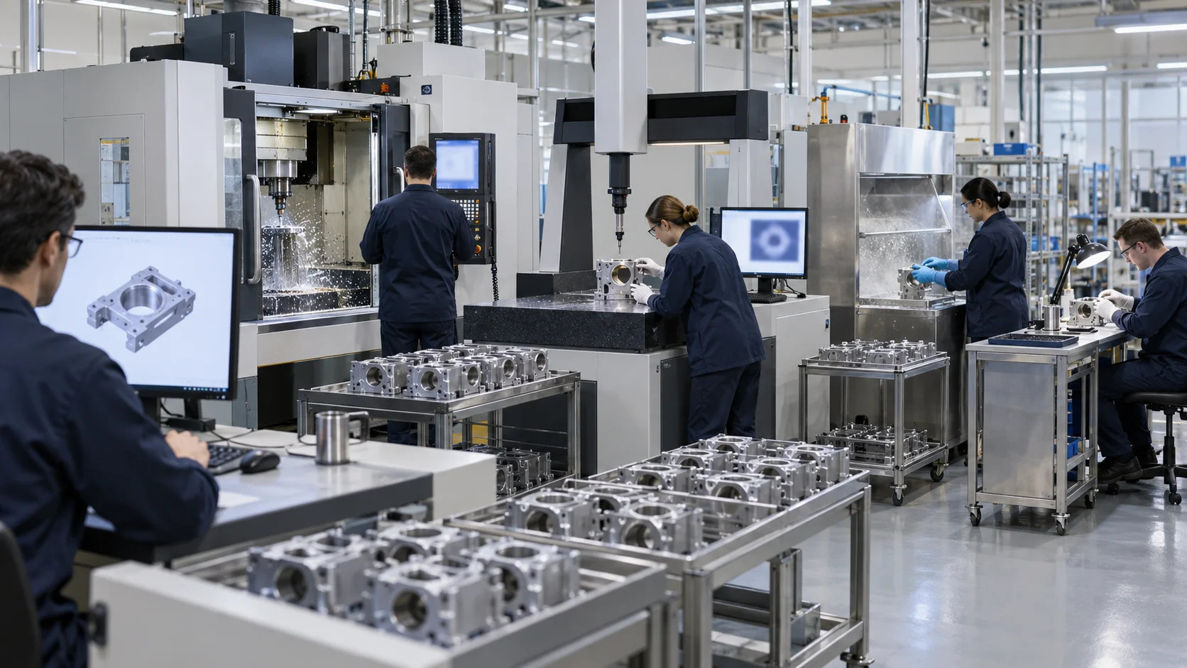
A practical process map connects engineering decisions to production controls. It normally includes requirement definition, design review, material selection, process planning, prototype manufacturing, inspection, finishing or cleaning, assembly, and controlled delivery. The sequence changes by part: a machined vacuum component does not follow exactly the same route as a formed enclosure or polymer fixture.
| Stage | What must be decided | Typical output |
|---|---|---|
| Requirements | Load, temperature, vacuum, chemical, cleanliness, and interfaces | Part specification |
| Design review | Datums, tolerances, wall thickness, access, and assembly | Released CAD and drawing |
| Process planning | Machining, sheet metal, molding, casting, or additive route | Manufacturing plan |
| Verifica | Dimensions, material, surface condition, and fit | Inspection record |
Start with the part requirements
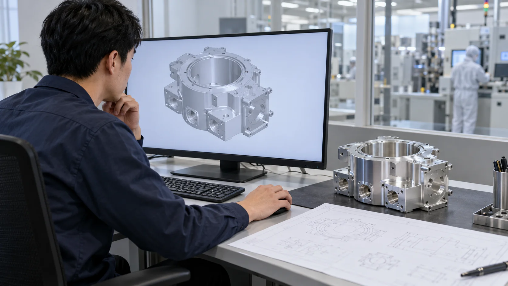
The first mistake in an equipment project is selecting a process before defining what the part must do. Review functional datums, sealing surfaces, locating features, fastener interfaces, thermal movement, and areas exposed to process chemicals or controlled environments.
Separate critical features from cosmetic preferences. Over-specifying every dimension can increase cost without improving performance, while an under-specified locating face or seal groove may create an assembly problem. A design-for-manufacturing review resolves these questions before material is purchased.
For the complete service scope, start with semiconductor equipment parts manufacturing and then match each requirement to a process capability.
Material choices follow the environment
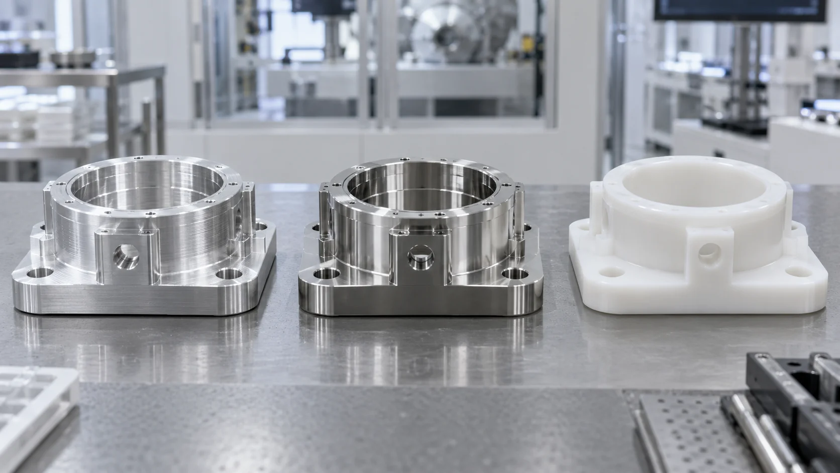
Material selection should follow the operating environment rather than a generic preference for aluminum, stainless steel, or plastic. Consider stiffness, thermal expansion, wear, corrosion resistance, outgassing concerns, electrical behavior, cleanability, and compatibility with the finishing route.
- Metals balance rigidity, machinability, corrosion behavior, and surface condition.
- Engineering plastics can support insulation, low-friction interfaces, guards, and fixtures when the environment permits.
- Specialist materials may be required when temperature, wear, or chemical exposure exceeds ordinary material limits.
Availability and verification matter as much as technical suitability. A grade that is difficult to source or certify can create risk in repeat production.
Match the process to the part
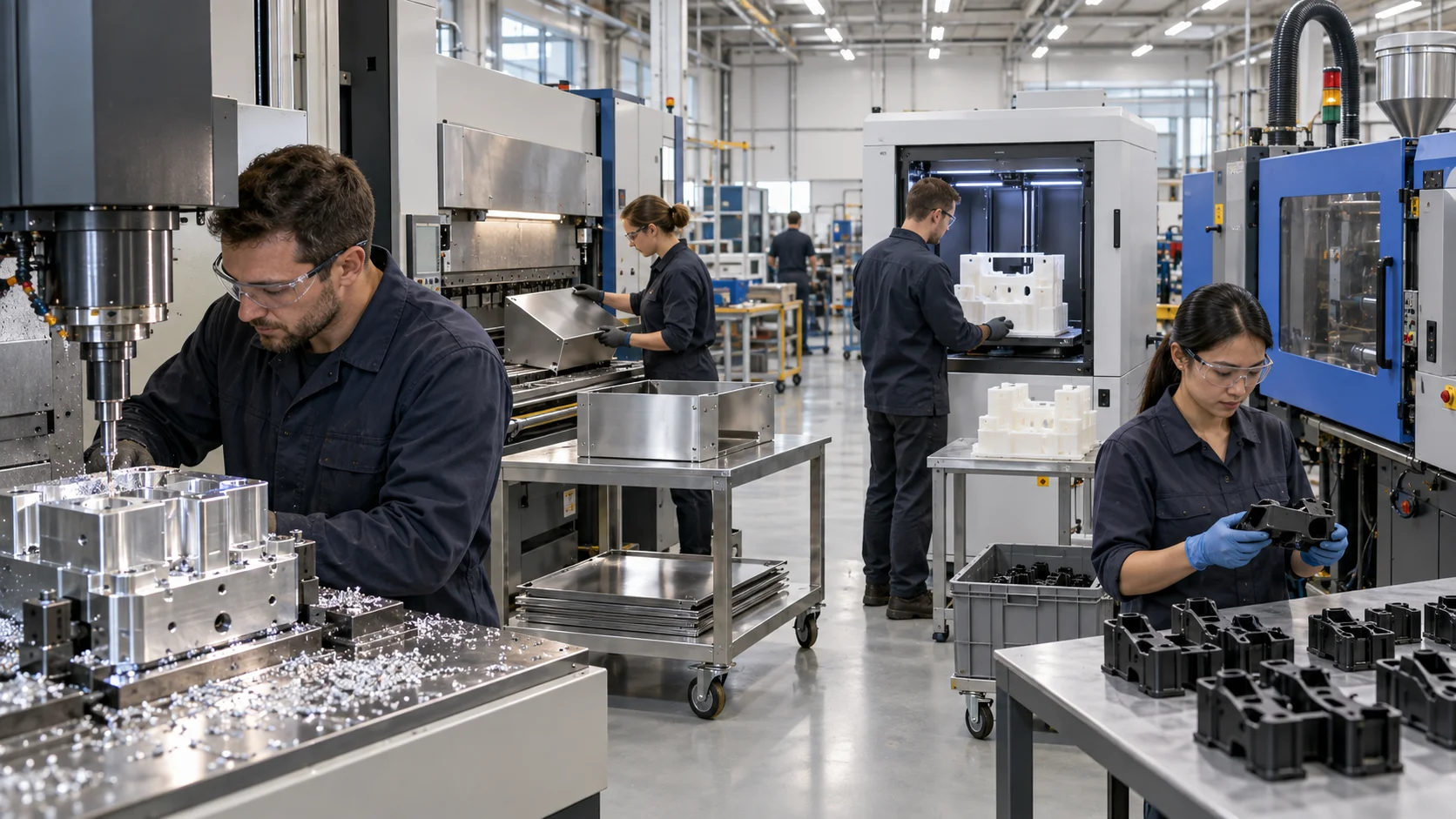
CNC machining is effective for tight interfaces, pockets, threads, and low-to-medium quantities. Sheet metal is efficient for cabinets, covers, panels, and structural enclosures. Additive manufacturing can accelerate complex prototypes, while molding or casting becomes attractive when geometry and volume justify tooling.
| Part situation | Often suitable route | Main review point |
|---|---|---|
| Tight-tolerance metal interface | La lavorazione CNC | Datum strategy and inspection access |
| Large protective enclosure | La fabbricazione della lamiera | Flatness, bends, access, and assembly |
| Complex early geometry | 3D printing or rapid prototyping | Functional fidelity and material limits |
| Repeated polymer housing | Injection molding or rapid tooling | Tooling investment and shrinkage |
Quality gates belong inside the flow
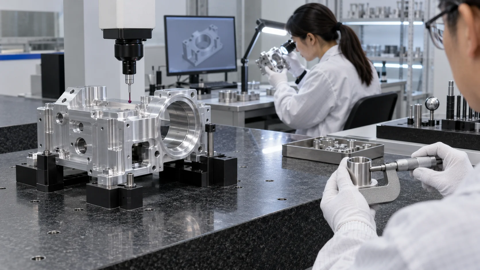
Quality should not be a single inspection at the end. Use checkpoints at drawing review, first article production, in-process machining, finishing, final inspection, and packing. Each checkpoint addresses a different risk: can the part be made, is the process stable, has the surface been altered correctly, and will the delivered part remain protected?
Evidence may include dimensional reports, material certificates, finishing records, photographs of identified features, and a packing checklist. The exact record should match the customer requirement and part risk.
The supplier handoff should be complete
Provide the latest drawing, 3D model, material, finish, quantity by build stage, critical dimensions, inspection expectations, and delivery destination. If the design is changing, identify frozen and open features.
A capable supplier should return questions that improve the design rather than accept ambiguous data. Clarifying a tolerance, surface callout, or packaging requirement early is less expensive than correcting a fit problem after assembly.
For repeat orders, retain the approved drawing revision, inspection method, finish requirement, and packaging instruction together. That record turns a one-time prototype decision into a usable manufacturing baseline.
Questions Engineers Ask About the Manufacturing Route
Do semiconductor manufacturing processes only refer to wafer fabrication?
No. In a component sourcing context, the phrase can also describe the manufacturing flow used to produce semiconductor equipment parts, structures, fixtures, enclosures, and assemblies.
Which process is best for equipment parts?
It depends on material, geometry, quantity, tolerance, surface requirement, and program stage. CNC machining, sheet metal, additive manufacturing, molding, and casting can each be appropriate.
The Engineering Takeaway
The most reliable process connects design intent, material behavior, production method, inspection, and delivery control. Treating these decisions as one system gives equipment teams a clearer path from concept to qualified, repeatable parts.